In this tutorial I hope to share how I made my new name tag, so others may learn and try it themselves! First off, I work at a Fab Lab, so I have many tools and software available for making. The software I used for my name tag are free to download; EAGLE by Autodesk, Inkscape, EASEL by Inventables, and Arduino. I used a Shapeoko CNC machine to mill my traces onto a thin PCB board. Hopefully you have access to a milling machine, if not you may have to try out a different method, like chemical etching. Ideally before beginning this project, you will have experience with milling, soldering, and uploading programs with Arduino software, as I don’t provide many details on how to do those tasks.

An expensive tool I used was my spark fun programmer, the red USB device shown above. This little guy allows me to put my Arduino code onto my ATtiny microcontroller. If you don’t want to invest $15 and you have an Arduino Uno laying around, you might use this tutorial instead! The main difference between all 8 pin ATtiny microcontrollers is how much memory they have available to use. Any 8 pin will do, but this tutorial is for the 25,45, or 85 versions. The example blink code uses only 678 bytes of memory so you could use an ATtiny13 too. I chose my 48 green LEDs for their low voltage drop(1.8 v), since I wasn’t keen on incorporating resistors in my design.

When installing a new font, it is best to select ‘Install for all Users’ instead of the regular “Install’ . This ensures that the Inkscape program will be able to locate and use it. Another thing to be aware of is that the font needs to be installed before opening Inkscape. If done while it is open, Inkscape won’t see it!

I opened Inkscape, changed my document properties to the size of my PCB board, and filled up the space with my name! In the document properties window, locate scale, and change your units before changing your numbers. Pro tip, a left finger on the Ctrl button on your keyboard and a right finger on the scroll of your mouse allows you to zoom in and out with ease. If you accidentally zoom out and lose your work space, press the number 5 to find it again!

If you have never used EAGLE before, have no fear! There are tons of great tutorials on how to install libraries and get started. Your library is your folder of electrical components, and most importantly their ‘footprint’ or ‘pads’. Some components are made to go completely through a circuit board, like my ATtiny. Others, like LEDs, just sit on top of it. It is important to make sure the parts you plan on using are the same parts in your folder. A surface mount ATtiny’s pads are much smaller than the bread board version, in EAGLE described as a ‘DIL08’. I used a library called “fab.lbr” to use my specific surface mount LEDs . To add a new downloaded library, make sure EAGLE is open to a new schematic, go to the top middle tab labeled ‘Library’, open your library manager, and locate your new library you want to use.


You have just created a path! Delete your original image and keep your path, select it, go to the top of Inkscape, click on ‘Path’, then select ‘Break Apart’. Separate the ATtiny pads from the resistor, delete the ATtiny holes/number pieces, then group the component’s pieces back together, but still separate from each other. Make sure you haven’t accidentally resized your component pads!

I find it helpful to change my font from ‘filled’ to just the ‘outline’, so I can easier arrange my LED pads. Select your font, go to the Fill and Stroke icon at the top of Inkscape. Once you have an outline, you can select your LED pads, press your Ctrl key and the ‘D’ key at the same time to quickly duplicate them.

Once you have spread out your LEDs you are ready to connect the pads to the ATtiny pads. In electronics jargon, these lines are called traces. They carry the electrical signals from the microcontroller to the LEDs. LEDs stand for Light Emitting Diodes, and all diodes are polarized, so electricity will only flow one direction. This means the negative traces should only ever touch the negative pin or pin 4 on the ATtiny. The positive traces I connected to the ‘instruction’ pin, in this case, I chose pin 5, 0, PWM. To determine what your pins are, Google any electrical component with the word pinout.


Creating two separate traces is tricky and may take a few tries. I recommend making them two different colors while designing. Once I had my traces all laid out I tweaked them here and there. To select an individual node, select the line you want to move, hit F2, and your nodes will appear. You can then individually select nodes to shift them around.


The best way to get a nice clean SVG file where all of the shapes are connected is to export the SVG as a a high, 600 DPI image. Immediately after exporting, open your image in Inkscape, select it, and press 3 keys at once, Shift, Alt, and the letter ‘B’ to open up the Trace Bitmap box. If you aren’t fond of keyboard shortcuts, you can also right click on the object, and select Trace Bitmap from the drop down menu.


Now it’s time to mill out your design! I will be using EASEL by Inventables to control my Shapeoko CNC machine. CNC stands for computer numerical control, meaning it’s simply following a path made up of numbers we created in our SVG. Create an account and select the EASEL tab from this page.


After changing your bit size and material you can begin by adjusting the path to be carved. On the left is your design, the right side shows how it will turn out on your material.

Ideally you will have used your milling machine before and will be familiar with the procedure of “homing” the bit in regards to your material. If not I recommend doing at least one simple practice project before milling out your name tag. A common issue is that the bed may not be perfectly even and flat, resulting in a unevenly milled board.


Your next task is to do a continuity test on your board. Make sure your negative traces and instruction pin traces are separate from each other before soldering your LEDs on. If there are any areas where they are touching, try to score the board with a small blade to separate them. I had to do that on two areas in my s’s.


You will definitely need a pair of tweezers at the point. Ideally you will already have experience with soldering. My approach was to cover the little pads with solder, place an LED in the correct orientation to the circuit. Solder one side, place a wee bit of pressure on the LED using the tweezers, and solder each side back and forth until the LED sinks flat onto the board. This takes some finesse, I promise it gets better with practice. There are other ways to solder SMT parts to circuit boards, a mask, solder paste, and oven or heat gun is an alternative way. In my experience however, LEDs are fickle things, give them too much heat and they will go pop! like a piece of corn. After every few LEDs I would test my circuit with a little coin cell battery. When testing, make sure you use a low voltage battery, too much electricity can also explode the LEDs. If you accidentally solder an LED the wrong way, it can be difficult to extract and turn it around. Be careful of pulling up your delicate little traces. A pro tip I’ve learned is to heat up the offending solder pad and quickly, firmly tap it onto the table top. This will make the excess solder fly off like water. This can be messy and a bit dangerous, so use caution and protect your eyes!


Once all of my LEDs were secured I plugged in my little 8 pin socket onto the board. Bend the little legs so it won’t fall out of the holes. I stripped my battery pack wires and wrapped them around my 5V and ground pins. Solder little blobs of solder to keep the wires from slipping off the pins. It is very important that two of those metal legs on your socket get soldered to the top ground and instruction pin traces. This is tricky and you might end up melting the socket a little bit like I did below...

When that is finished you are ready to program your ATtiny, in my case, an ATtiny45! We have to first make sure the Arduino knows how to ‘talk’ to the ATtiny, by installing a special driver. Follow this lovely tutorial to install the board/driver files for the ATtinys. In addition to a board library for Arduino, you may need to install a driver for your sparkfun programmer. Once those two items are taken care of you should be able to program your ATtinys with ease! I used the basic example program called ‘Blink’. The only adjustment I had to do was change the LED_BUILTIN to ‘0’, our instruction pin on the ATtiny.

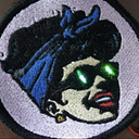
Once you have uploaded your code, you can plug your ATtiny into the socket, place some coin cell batteries into your battery holder, secure your battery holder and pin device to the back of the PCB(I used foam tape) and you are ready to rock your new blinky name tag!

Good luck with your own blinky badge, please don’t hesitate to ask me questions!